Building and manipulating 3-D and linked 2-D structures of nanoparticles using scanning force microscopy
R. Resch, C. Baur, A. Bugacov, B.E. Koel†, A. Madhukar, A.A.G. Requicha, P. Will
Laboratory for Molecular Robotics, University of Southern California.
947 West 37th Place, Los Angeles, CA 90089-0781, U.S.A.
Telephone: +1 (213) 740-4502
Fax: +1 (213) 740-7512
E-mail: lmr@lipari.usc.edu
† Department of Chemistry, University of Southern California.
920 W. 37th Street, University Park, Los Angeles, CA 90089-0482, U.S.A.
Telephone: +1-213-740-4126
Fax: +1-213-740-3972
E-mail: koel@chem1.usc.edu
Abstract
Manipulation of nanoparticles with the atomic force microscope (AFM) has been limited until now to clearing areas on a surface, or to moving single particles sequentially to create 2-D patterns. The research reported here uses a previously described setup for nanomanipulation with the AFM to (i) build a simple 3-D pyramidal structure by pushing a nanoparticle on top of two others, and (ii) rotate and translate a linked two-particle structure. The experiments are conducted in air and at room temperature with gold nanoparticles deposited on silicon previously coated with a silane layer.
1. Introduction
Nanoparticles and structures formed of nanoparticles have physical properties different from those of the bulk materials. They exhibit phenomena such as the quantization of energy, charge and conductance [1-3] which and may lead the way to future nanodevices such as single-electron transistors [4]. However, many of the potential applications will require the precise positioning of nanoparticles in complex two- and three-dimensional structures. Several methods have been proposed to construct such structures [5-7]. Another promising strategy is using the tip of a scanning force microscope (SFM) to manipulate nanoparticles on surfaces [8-12]. Usually, a linescan including the nanoparticle and its desired position is taken before manipulation with the SFM operated in dynamic mode (non-contact or intermittent contact). During manipulation either the feedback is switched off [9,11,12] or the SFM is operated in static mode (full contact) [8,10] and the particle is moved by the tip to its new position on a surface. Until now only a few groups have reported precise positioning of nanoparticles to form two-dimensional structures on the surface by using an SFM [8-14]. However, there have been no previous reports of building two-dimensional structures or units out of single nanoparticles which could then later be manipulated as a whole unit. This requires not only contact between the particles but also connection. Building a three-dimensional structure out of single nanoparticles has also not yet been demonstrated. In this paper, we present both the preparation of a pyramid-like structure, as an example of construction of a three-dimensional structure by manipulation of single nanoparticles, and the manipulation of a dimer unit formed by two linked nanoparticles.
2. Experimental Section
The sample was prepared by depositing gold colloidal particles (EM.GC15; Ted Pella Inc.) with diameters of 15 nm and 30 nm from aqueous solutions on a silicon surface that had been previously coated with a film of Aminopropyltrimethoxysilane (APTS) (Z-6020 Silane; Dow Corning). Prior to depositing of the nanoparticles, the silicon substrate was rinsed with concentrated sulfuric acid, deionized water, acetone and methanol. In order to deposit the layer of APTS, the Si substrate was dipped for 1 hour in an aqueous solution of 1% APTS containing 1×10⁻³ M acetic acid. Subsequently, the samples were annealed in air for 5 min at 120C.
Imaging and pushing experiments were carried out with an Autoprobe CP AFM (Park Scientific Instruments) operated in non-contact mode in air using triangularly shaped silicon cantilevers (Park Scientific Instruments, spring constant: 13.0 Nm-1, resonance frequency: 340 kHz).
Manipulation of the nanoparticles was performed by utilizing the Probe Control Software (PCS) which was developed in our group [12] and is built upon the application programming interface provided by Park Scientific Instruments. This software allows the user to take single linescans by setting an ìarrowî in a previously recorded non-contact mode image. The arrow determines the direction and length of the subsequent scanline and can be moved by the operator in the x- and y-direction until the displayed topography indicates that its path is centered over the particle. In order to compensate for relative position drifts, a tracking tool based on the differential height between the particle and the surface can be activated to keep the arrow going through the center of the particle. Two bars can be positioned along the scanline within which alternative operating conditions of the AFM and therefore the ìstartî and ìendî points of the manipulation can be selected. In this study the feedback was turned off just before the tip was scanned across the particle and switched back on after reaching the desired lateral position. Furthermore, the software allows access to various signals such as the deflection and the amplitude of the cantilever during manipulation. By analyzing these data we have previously shown that the particles are pushed across the surface and studied the underlying mechanics of the pushing operation [15].
3. Results
The series of topview images presented in figure 1 shows the preparation of a pyramid-like structure by pushing one nanoparticle up between two others. Figure 1A shows the topography of a region of the sample before manipulation. The scan area is 600 nm x 400 nm. Three particles with a diameter of 30 nm and marked with the numbers 1,2 and 3 can be observed among several particles with diameters of 15 nm. The arrow indicates the direction of the manipulation operation and the two perpendicular bars specify the region where the feedback was turned off. Figure 1B records the result of the manipulation operation indicated by the arrow in Figure 1A. Particle 1 was pushed between particle 2 and 3 forming a pyramid-like structure. After forming the 3D-structure particle 1 was pushed away from particle 2 and 3 as indicated by the arrow in figure 1B and isolated again (figure 1C).
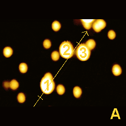
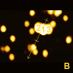
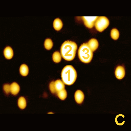
Fig.1 A-C: Pushing of a gold nanoparticle (1) with a diameter of 30 nm up and between two others (2 and 3) and back. Figure 1A shows an AFM image of the surface area before manipulation and figure 1B the AFM image of the same area after pushing particle 1 between 2 and 3 as indicated by the arrow in figure 1A. Figure 1C shows the AFM image after particle 1 was isolated again. The scan area is 450 nm x 300 nm.
The 3-D structure is more clearly revealed in figure 2. Figure 2A shows a topview of the pyramidal structure. Figures 2B and 2C show the line scans of the two orthogonal lines in figure 2A. Both line scans reveal that particle 1 is now elevated about 20 nm, and sitting between particles 2 and 3. This is the first report of a 3-D structure built from single nanoparticles using an AFM.

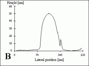
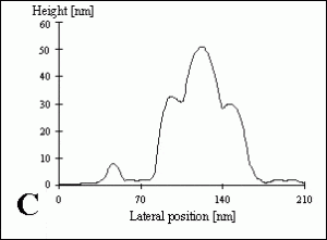
Figure 2 A-C: Elevation of particle 1 after being pushed up and between particles 2 and 3. Figures 2B and 2C show the two orthogonal line scans as indicated in figure 2A. Elevation of particle 1 after being pushed up and between particles 2 and 3. Figures 2B and 2C show the two orthogonal line scans as indicated in figure 2A.
Similar experiments on particles deposited on mica that was covered with a poly-L-lysine film showed different results. Instead of achieving a 3D-structure by pushing one particle on top of two others, all three of the particles moved producing a new arrangement of the particles on the surface. This is in excellent agreement with our observations that a single particle deposited on a poly-L-lysine film can be moved with a different set of operating parameters for the AFM than a particle deposited on an APTS film. Obviously, the interaction between a gold nanoparticle and the silane layer is stronger than between a gold nanoparticle and the poly-L-lysine layer. These observations show that building 3D-structures of single particles requires careful selection of an appropriate underlayer, in addition to a precise manipulation process.
Figure 3 shows a sequence of manipulation stages of two particles attached to each other forming a dimer. The motion of this unit depends on where the two particle assembly is pushed. Again, the arrow in each image indicates the scan line along which the manipulation operation was subsequently performed, and the two bars on these arrows define the length over which the feedback was turned-off. Then, the following image in the sequence represents the result of the manipulation indicated by the arrow and the bars in the prior image.
After several manipulation operations including repetitions of the experiment discussed in figure 1, we observed that particles 1 and 2 had been connected to each other forming a unit (figure 3A). A common strategy to form connections between gold nanoparticles in a monolayer is to use dithiols [16,17]. Since we were able to repeatedly form connections between gold particles deposited on APTS films, these experiments might reveal a new strategy for the connection of gold nanoparticles. Although we do not precisely know the nature of the connection, an explanation for its origin might be that one of the “bumps” which can also be observed on the surface is acting like a connector. These “bumps” are polymerized APTS. Since the APTS layer forms selectively strong bonds with the gold nanoparticles, it is quite possible that the polymerized APTS structure act like “glue”.
Figure 3B shows the image taken after the dimer was pushed as indicated by the arrow in figure 3A revealing that the whole unit was precisely moved across the surface. The sequence of images shown in figure 3B to figure 3G reveal that the dimer can be not only precisely moved over a given length, but also precisely rotated. Figure 3C shows the result of the pushing operation indicated by the arrow in figure 3B. Because of the connection to particle 1, the position of particle 2 was only changed slightly. Instead of translating the whole unit, it was rotated around particle 1 when particle 2 was pushed by the tip. Figures 3D and 3E display the result of subsequent manipulations of particle 2 as indicated by the arrows in figures 3C and 3D, respectively. The unit remained connected and was further rotated around particle 1. With the next two pushing operations particle 1 was pushed as indicated by the arrows in figures 3E and 3F. This demonstrates that the unit could also be rotated around particle 2 as shown in figures 3F and 3G). In the final manipulation, shown in figure 3H, the dimer was pushed towards particle 3 as indicated by the arrow in figure 3G to form a triangular-shaped structure with particle 3.
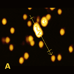
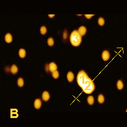
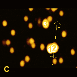
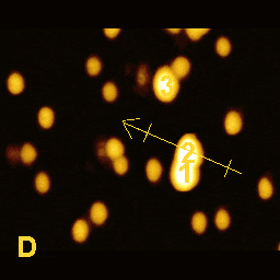
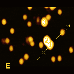
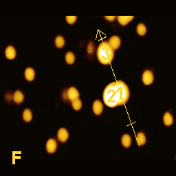
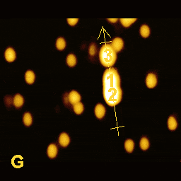
Figure 3 A-H: A sequence of 450 nm by 350 nm AFM images showing the manipulation of a unit (dimer) of two particles 1 and 2 attached to each other. The motion depends on where the two-particle assembly is pushed. The arrows indicate the manipulation operation whose result is recorded in the following image. Figure 1A shows the particles before manipulation. Figures 1B and 1H show a translational motion of the unit across the surface, whereas figures 1C-1E display rotations of the dimer around particle 1. Figures 1F and 1G show rotations of the dimer around particle 2.
4. Concluding remarks
The results presented here greatly extend the previously reported capabilities for the manipulation of nanoparticles using the tip of a scanning force microscope under ambient conditions in two new directions. We have demonstrated the construction of a 3-D structure by controlled manipulation of single nanoparticles. Furthermore, we have shown that single nanpoparticles can be connected to each other to form simple structures such as a dimer consisting of two nanoparticles. These structures can be precisely translated by mechanical pushing of the unit across the surface or rotated about a specific axis. These results offers new possibilities for constructing nanoscale 2-D and even 3-D structures.
5. Acknowledgements
This research was supported by the Z.A. Kaprielian Technology Innovation Fund.
Literature
[1] D.C. Ralph, C.T. Black, and M. Tinkham, Phys. Rev. Lett. 74, 3241 (1995)
[2] L. Giaever and H.R. Zeller , Phys. Rev. Lett. 20, 1504 (1968)
[3] C.J. Muller, J.M. v. Ruitenbeck, and L.J. de Jongh, Phys. Rev. Lett. 69, 140 (1992)
[4] P.C. Hidber, P.F. Nealey, W. Helbig, and G.M. Whitesides, Langmuir 12, 1375 (1996)
[5] H. Ahmed, J. Vac. Sci. Technol. A 14, 1178 (1996)
[6] F.K. Perkins, E.A. Dobisz, S.L. Brandow, J.M. Calvert, J.E. Kosakowski, and C.R.K. Marrian, Appl. Phys. Lett. 68, 550 (1996)
[7] P.C. Ohara, J.R. Heath, and W.M. Gelbart, Angew. Chemie Int. Ed. Engl. 36, 1077 (1997)
[8] D.M. Schaefer, R. Reifenberger, A. Patil, and R.P. Andres, Appl. Phys. Lett. 66, 1012 (1995)
[9] T. Junno, K. Deppert, L. Montelius, and L. Samuelson, Appl. Phys. Lett. 66, 3627 (1995)
[10] P. Sheehan and C.M. Lieber, Science 272, 1158 (1996)
[11] S.L. Brandow, W.J. Dressick, C.S. Dulcey, T.S.Koloski, L.M. Shirey, J. Schmidt, and J.M. Calvert, J. Vac. Sci. Technol. B 15, 1818 (1997)
[12] C. Baur, B.C. Gazen, B.E. Koel, T.R. Ramachandran, A.A.G. Requicha, and L. Zini, J. Vac. Sci. Technol. B 15, 1577 (1997)
[13] A.A.G. Requicha, C. Baur, A. Bugacov, B.C. Gazen, B.E. Koel, A. Madhukar, T.R. Ramachandran, and R. Resch, Proc. IEEE Intíl Conf. on Robotics & Automation, Leuven, Belgium, 136 (1998),
[14] T. R. Ramachandran, C. Baur, A. Bugacov, A. Madhukar, B.E. Koel, A.A.G. Requicha, and B.C. Gazen, accepted for publication in Nanotechnology (1998)
[15] R. Resch, C. Baur, A. Bugacov, B.C. Gazen, B.E. Koel, A. Madhukar, T.R. Ramachandran , A.A.G. Requicha, and P. Will, Appl. Phys. A (1998), in press
[16] T. Sato and H. Ahmed, Appl. Phys. Lett 70, 2750 (1997)
[17] R.P. Andres, J.D. Bielefeld, J.L. Henderson, D.B. Janes, V.R. Kolagunta, C.P. Kubiak, W.J. mahoney, and R.G. Osifchin, Science 273, 1690 (1996)