Nanorobotics is an emerging field that deals with the controlled manipulation of objects with nanometer-scale dimensions. Typically, an atom has a diameter of a few Ångstroms (1 Å = 0.1 nm = 10-10 m), a molecule’s size is a few nm, and clusters or nanoparticles formed by hundreds or thousands of atoms have sizes of tens of nm. Therefore, Nanorobotics is concerned with interactions with atomic- and molecular-sized objects-and is sometimes called Molecular Robotics. We use these two expressions, plus Nanomanipulation, as synonyms in this article.
Molecular Robotics falls within the purview of Nanotechnology, which is the study of phenomena and structures with characteristic dimensions in the nanometer range. The birth of Nanotechnology is usually associated with a talk by Nobel-prize winner Richard Feynman entitled “There is plenty of room at the bottom”, whose text may be found in [Crandall & Lewis 1992]. Nanotechnology has the potential for major scientific and practical breakthroughs. Future applications ranging from very fast computers to self-replicating robots are described in Drexler’s seminal book [Drexler 1986]. In a less futuristic vein, the following potential applications were suggested by well-known experimental scientists at the Nano4 conference held in Palo Alto in November 1995:
- Cell probes with dimensions ~ 1/1000 of the cell’s size
- Space applications, e.g. hardware to fly on satellites
- Computer memory
- Near field optics, with characteristic dimensions ~ 20 nm
- X-ray fabrication, systems that use X-ray photons
- Genome applications, reading and manipulating DNA
- Nanodevices capable of running on very small batteries
- Optical antennas
Nanotechnology is being pursued along two converging directions. From the top down, semiconductor fabrication techniques are producing smaller and smaller structures-see e.g. [Colton & Marrian 1995] for recent work. For example, the line width of the original Pentium chip is 350 nm. Current optical lithography techniques have obvious resolution limitations because of the wavelength of visible light, which is in the order of 500 nm. X-ray and electron-beam lithography will push sizes further down, but with a great increase in complexity and cost of fabrication. These top-down techniques do not seem promising for building nanomachines that require precise positioning of atoms or molecules.
Alternatively, one can proceed from the bottom up, by assembling atoms and molecules into functional components and systems. There are two main approaches for building useful devices from nanoscale components. The first is based on self-assembly, and is a natural evolution of traditional chemistry and bulk processing-see e.g. [Gómez-López et al. 1996]. The other is based on controlled positioning of nanoscale objects, direct application of forces, electric fields, and so on. The self-assembly approach is being pursued at many laboratories. Despite all the current activity, self-assembly has severe limitations because the structures produced tend to be highly symmetric, and the most versatile self-assembled systems are organic and therefore generally lack robustness. The second approach involves Nanomanipulation, and is being studied by a small number of researchers, who are focusing on techniques based on Scanning Probe Microscopy (abbreviated SPM, and described later in this article).
A top-down technique that is closely related to Nanomanipulation involves removing or depositing small amounts of material by using an SPM. This approach falls within what is usually called Nanolithography. SPM-based Nanolithography is akin to machining or to rapid prototyping techniques such as stereolithography. For example, one can remove a row or two of hydrogen atoms on a silicon substrate that has been passivated with hydrogen by moving the tip of an SPM in a straight line over the substrate and applying a suitable voltage. The removed atoms are “lost” to the environment, much like metal chips in a machining operation. Lines with widths in the order of 10 to 100 nm have been written by these techniques-see e.g. [Wiesendanger 1994] for a survey of some of this work. In this article we focus on Nanomanipulation proper, which is akin to assembly in the macroworld.
Nanorobotics research has proceeded along two lines. The first is devoted to the design and computational simulation of robots with nanoscale dimensions-see [Drexler 1992] for the design of robots that resemble their macroscopic counterparts. Drexler’s nanorobot uses various mechanical components such as nanogears built primarily with carbon atoms in a diamondoid structure. A major issue is how to build these devices, and little experimental progress has been made towards their construction.
The second area of Nanorobotics research involves manipulation of nanoscale objects with macroscopic instruments. Experimental work has been focused on this area, especially through the use of SPMs as robots. The remainder of this article describes SPM principles, surveys SPM use in Nanomanipulation, looks at the SPM as a robot, and concludes with a discussion of some of the challenges that face Nanorobotics research.
Scanning Probe Microscopes
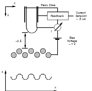
The Scanning Tunelling Microscope (STM) was invented by Binnig and Rohrer at the IBM Zürich laboratory in the early 1980s, and won them a Nobel prize four years later. The principles of the instrument can be summarized with the help of Figure 1.
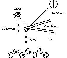
Various instruments analogous to the STM have been built. They exploit physical properties other than the tunneling effect on which the STM is based. The most common of these other instruments is the Atomic Force Microscope (AFM), which is based on interatomic forces. All of these instruments are collectively known as Scanning Probe Microscopes (SPMs). The principles of operation of the AFM are shown in Figure 2. The forces between atoms in the tip and sample cause a deflection of the cantilever that carries the tip. The amount of deflection is measured by means of a laser beam bouncing off the top of the cantilever. (There are other schemes for measuring deflection.) The force depends on the tip/sample gap, and therefore servoing on the force ensures that the distance is kept constant while scanning, as in the STM. The AFM does not require conducting tips and samples, and therefore has wider applicability than the STM.
For more information on SPM technology see for example [Wiesendanger 1994]. Although the SPM is not even twenty years old, it has had a large scientific impact. There is a voluminous literature on SPM applications, scattered through many journals such as Science and the Journal of Vacuum Science and Technology, and proceedings of meetings such as the biennial conference on Scanning Tunneling Microscopy.
Nanomanipulation with the SPM
Since the early days of the SPM it was known that tip/sample interaction could produce changes in both tip and sample. Often these were undesirable, for example, a blunt probe due to a crash into the sample. But it soon became clear that one could produce new and desirable features on a sample by using the tip in a suitable manner. One of the first demonstrations was done by Becker and co-workers at Bell Labs, who managed to create nanometer-scale germanium structures on a germanium surface by raising the voltage bias of an STM tip [Becker et al. 1987]. Much of the subsequent work falls under the category of Nanolithography and will not be discussed here. In the following subsections we survey Nanomanipulation research involving the SPM.
Pushing and Pulling
Pushing and pulling operations are not widely used in macrorobotics, although there has been interesting work on orienting parts by pushing, done by Matt Mason at CMU, Ken Goldberg at USC, and others. The techniques seem suitable for constructing 2-D structures.
Interatomic attractive forces were used by Eigler et al. at IBM Almadén to precisely position xenon atoms on nickel, iron atoms on copper, platinum atoms on platinum, and carbon monoxide molecules on platinum [Stroscio & Eigler 1991]. The atoms are moved much like one displaces a small metalic object on a table by moving a magnet under the table. The STM tip is placed sufficiently close to an atom for the attractive force to be larger than the resistance to lateral movement. The atom is then pulled along the trajectory of the tip. Eigler’s experiments were done in ultra high vacuum (UHV) at very low temperature (4K). Low temperature seems essential for stable operation. Thermal noise destroys the generated patterns at higher temperatures.
Lateral repulsive forces were used by Güntherodt’s group at the University of Basel to push fullerene (C60) islands of ~ 50nm size on flat terraces of a sodium chloride surface, in UHV, at room temperature, with a modified AFM [Lüthi et al. 1994]. The ability to move the islands depends strongly on species/substrate interaction, e.g., C60 does not move on gold, and motion on graphite destroys the islands. Lateral forces opposing the motion are analogous to friction in the macroworld, but cannot be modeled simply by Coulomb friction or similar approaches that are used in macrorobotics.
Mo at IBM Yorktown rotated pairs of antimonium atoms between two stable orientations 90 degrees apart [Mo 1993]. This was done in UHV at room temperature, on a silicon substrate, by scanning with an STM tip with a higher voltage than required for imaging. The rotation was reversible, although several scans were sometimes necessary to induce the desired motion.
Samuelson’s group at the University of Lund succeeded in pushing galium arsenide (GaAs) nanoparticles of sizes in the order of 30 nm on a GaAs substrate at room temperature in air [Junno et al. 1995]. The sample is first imaged in non-contact AFM mode. Then the tip is brought close to a nanoparticle, the feedback is turned off and the tip is moved against the nanoparticle. Schaefer et al. at Purdue University push gold clusters with an AFM in a nitrogen environment at room temperature [Schaefer et al. 1995]. They first image the clusters in non-contact mode, then remove the tip oscillation voltage, and sweep the tip across the particle in contact with the surface and with the feedback disabled.
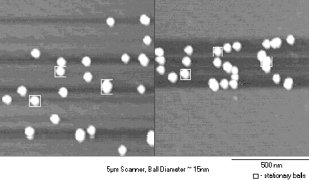
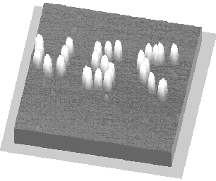
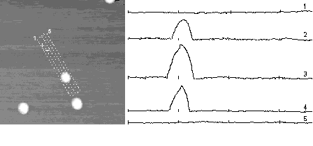
A similar technique is being used at USC’s Laboratory for Molecular Robotics to push colloidal gold nanoparticles with 15 nm diameters on a mica substrate at room temperature and in ambient air. We image in non-contact mode, then disable the feedback and push by moving the tip in a single line scan, without removing the tip oscillation voltage. Figure 3 shows on the right a “USC” pattern written with gold nanoparticles. The z coordinate is encoded as brightness in this figure. On the left is the original random pattern, before manipulation with the AFM. Figure 4 shows the same “USC” pattern displayed in perspective. A 3-D VRML (Virtual Reality Modeling Language) file, obtained from the terrain map shown in Figure 3 is available for browser viewing by following the “What’s Cool” link in http://www-lmr.usc.edu/~lmr.
Smaller objects have been arranged into prescribed patterns at room temperature by Gimzewski’s group at IBM’s Zürich laboratory. They push molecules at room temperature in UHV by using an STM. They have succeeded in pushing porphyrin molecules on copper [Jung et al. 1996], and more recently they have arranged bucky balls (i.e., C60) in a linear pattern, using an atomic step in the copper substrate as a guide [Cuberes et al. 1996].
C60 molecules on silicon also have been pushed with an STM in UHV at room temperature by Maruno et al. in Japan [Maruno et al. 1993], and Beton et al. in the U.K. [Beton et al. 1995]. In Maruno’s approach the STM tip is brought closer to the surface than in normal imaging mode, and then scan across a rectangular region with the feedback turned off. This causes many probe crashes. In Beton’s approach the tip also is brought close to the surface, but the sweep is done with the feedback on and a high value for the tunneling current. Their success rate is in the order of only 1 in 10 trials.
Much of industrial macrorobotics is concerned with pick and place operations, which typically do not require very precise positioning or fine control. There are a few examples of experiments in which atoms or molecules are transferred to SPM tips, these are moved, and the atoms transferred back to the surfaces.
Eigler et al. succeeded in transferring xenon atoms from platinum or nickel surfaces to an STM tip by moving the tip sufficiently close for the adsorption barriers of surface and tip to be comparable [Stroscio & Eigler 1991]. An atom may leave the surface and become adsorbed to the tip, or vice-versa. Benzene molecules also have been transferred to and from tips.
Eigler’s group also has been able to transfer xenon atoms between an STM tip and a nickel surface by applying voltage pulses to the tip [Stroscio & Eigler 1991]. This is attributed to electromigration, caused by the electric current flowing in the tunneling junction. All of Eigler’s work has been done in UHV at 4K.
Avouris’ group, at IBM Yorktown, and the Aono group in Japan have transferred silicon atoms between a tungsten tip and a silicon surface in UHV at room temperature, by applying voltage pulses to the tip [Lyo & Avouris 1991] [Uchida et al. 1993]. The mechanism for the transfer is believed to be field-induced evaporation, perhaps aided by chemical phenomena at the tip/surface interface in Avouris work.
Compliant Motion
This is the most sophisticated form of macrorobotic motion. It involves fine motions, as in a peg-in-hole assembly, in which there is accomodation and often force control, for example to ensure contact between two surfaces as they slide past each other. Compliance is crucial for successful assembly operations in the presence of spatial and other uncertainties, which are unavoidable.
The study of the nanoscale analog of compliant motion seems to be virgin territory. We speculate that the analog of compliance is chemical affinity between atoms and molecules. We suspect that such “chemical compliance” may prove essential for nanoassembly operations at room temperature, in the presence of thermal noise. It seems likely that successful assembly of nanoscale components will require a combination of precise positioning and chemical compliance. Therefore, work on self-assembling structures is relevant.
The SPM as a Robot
Motion
To first approximation, an SPM is a 3 degree-of-freedom robot. It can move in x, y, and z, but cannot orient its tip, which is the analog of a macrorobotic hand. (How could a 6 degree-of-freedom SPM be built, and what could be done with it, are interesting issues.) The vertical displacement is controlled very accurately by a feedback loop involving tunneling current or force (or other quantities for less-common SPMs). But nanoscale x,y motion over small regions (e.g., within a 5 micron square) is primarily open-loop, because of a lack of suitable sensors that can be used in a feedback scheme. Accurate horizontal motion relies on calibration of the piezoelectric actuators, which are known to suffer from a variety of problems such as creep and hysteresis. In addition, thermal drift of the instrument is very significant. At room temperature a drift of one atomic diameter per second is common, which means that manipulation of atomic objects on a surface is not unlike picking parts from a conveyor belt. Thermal drift is negligible if the SPM is operated at very low temperatures, and all the experiments in atomic-precision manipulation to date have been done at 4K. This involves complex technology and is clearly undesirable. For room-temperature nanomanipulation, drift, creep and hysteresis must be taken into account. Ideally, compensation should be automatic. Research is under way at USC on how to move accurately an SPM tip in the presence of all these sources of error.
To complicate matters further, the SPM often must operate in a liquid environment, especially if the objects to be manipulated are biological. Little is known about nanomanipulation in liquids.
Sensing
The SPM functions both as a manipulator and a sensing device. The lack of a direct and independent means of establishing “ground truth” while navigating the tip causes delicate problems. The SPM commands are issued in instrument or robot coordinates, and sensory data also are acquired in robot coordinates, whereas manipulation tasks are expressed in sample or task coordinates. These two coordinate systems do not coincide, and indeed are in relative motion due to drift. Accurate motion in task coordinates may be achieved by a form of visual servoing, by tracking features of the sample and moving relative to them.
A simple example of a practical implementation of these ideas is illustrated in Figure 5. To construct the pattern shown in Figures 3 and 4 we move the tip to the approximate position of a nanoparticle to be pushed, and then search for it through single-line scans.
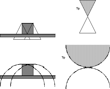
The SPM output signal depends not only on the topography of the sample but also on the shape of the tip, and on other characteristics of the tip/sample interaction. For example, the tunneling current in an STM depends on the electronic wavefunctions of sample and tip. To first approximation one may assume that the tip and sample are in contact. Under this assumption one can use configuration-space techniques to study the motion of the tip [Latombe 1991]. Figure 6 illustrates the procedure in 2-D. On the top of the figure we consider a tip with a triangular end and a square protrusion in the sample. In the bottom we consider a tip with a semi-circular end and the same protrusion. We choose as reference point for the tip its apex, and reflect the tip about the reference point. The configuration-space obstacle that corresponds to the real-space protrusion obstacle is obtained by sweeping the inverted tip over the protrusion so that the apex remains inside the obstacle. Mathematically, we are calculating the Minkowski sum of the inverted tip and the protrusion. The path of the tip in its motion in contact with the obstacle is the detected topographical signal. As shown in the figure, the sensed topography has been broadened by the dimensions of the tip. Note, however, that the detected height is correct. (Minkowski operations and related mathematical morphology tools were introduced in the SPM literature only recently [Villarrubia 1994].) Tip effects are sometimes called “convolution”, by analogy with the broadening of an impulse passing through a linear system, and one talks of “deconvolving” the image to remove tip effects.
A major issue in tip-effect compensation is that the shape of the probe is not known, and indeed may vary during operation. For example, atoms may be adsorbed on the tip or lost because of the contact with the sample. The most promising approach for dealing with tip effects consists of estimating the tip shape by using it to image known features. If necessary, artificial features may be introduced into the scene for tip estimation purposes. The estimated tip shape can then be used to remove (at least in part) the tip effects from the image by using Minkowski operations [Villarrubia 1994]. Removal procedures that take into account more sophisticated, non-geometric effects, do not appear to be known.
Sensor fusion techniques may be used, at least in principle, for increasing the quality of the sensory data, because it is possible to access several signals during an SPM scan. For example, vertical and lateral force (akin to friction) can be recorded simultaneously in typical AFMs. To our knowledge, sensor fusion has not been attempted in SPM technology.
It is clear that faithful sensory data should facilitate manipulation tasks. What is not clear is whether clever manipulation strategies can compensate for the imperfections of SPM data.
End Effectors
The SPM tip is the primary end effector in nanomanipulation. A plain, sharp tip seems to be adequate for most pushing operations. In some cases it may also suffice for picking and depositing objects, especially in conjunction with electrostatic forces generated by applying a suitable bias to the tip. This requires both a conducting tip and a conducting substrate. Pick-and-place tasks, however, usually require the nanoscale analog of a gripper. Very little is known about molecular grippers.
One can think of a nanogripper as a molecule or cluster of molecules that are attached to a tip and are capable of picking up and transporting other molecules or particles. (Tips with attached molecules are said to be functionalized.) Ideally these grippers should be switchable, so as to pick and release objects on command. Candidates for grippers are certain molecules such as cyclodextrins, which have large cavities that can carry other molecules. Coating a tip with strands of DNA may also permit picking up objects that are coated with complementary strands. In both of these examples, switching the gripper on and off is not a solved problem.
Techniques for changing SPM tips automatically do not exist. Changes must be done manually, and it is very difficult or impossible to maintain sample registration, i. e., to return to the same position on the sample after tip replacement. This implies that one often must image using a tip with an attached gripper. Again, little is known about imaging with such functionalized tips.
Fixtures
In the macroworld fixtures are often necessary to hold mechanical parts during assembly and other manufacturing operations. In micromechanics sacrificial layers are used as scaffolding to fabricate certain microelectromechanical systems (MEMS). At the nanoscale, the analogs of fixtures are substrates that ensure that certain objects remain fixed during manipulation, while others are allowed to move. Substrate selection seems to be highly dependent on the chemistry of the objects being manipulated.
Manipulation Processes
In macrorobotics the physical processes involved are mechanical and relatively well understood. At the nanoscale, the processes are chemical and physical, and still an area of active research. In addition, nanomanipulation takes place in several different environments, such as liquids, air or UHV. The environment has a strong influence on the physics and chemistry of the processes. Nanomanipulation is not restricted to mechanical interactions. For example, light, electrostatic fields, and the pH of a liquid all are candidates for controlled interaction with nanoparticles.
Programming and Planning
High level programming and planning systems are highly desirable, and indeed essential for assembling complex structures. One must begin with relatively low-level programming primitives and build upon them constructs at a higher level of abstraction. High-level commands must be compiled into low-level primitives. This compilation may involve sophisticated computations, for example to ensure collision-free paths in an environment with large spatial uncertainty. What are the relevant high-level manipulation tasks? For example, what is the nanoscale equivalent of a peg-in-hole insertion? In short, we may need to adapt much of what is known about macrorobotics to the nanoworld. It is likely that new concepts will also be needed, because the physics and chemistry of the phenomena and objects are quite different in these two worlds.
Assembly Applications
What hardware primitives are suitable as building blocks? The nanotechnology literature suggests hardware primitives based on DNA structures such as those built in Seeman’s lab [Seeman et al. 1993], proteins, and diamondoid structures [Drexler 1992]. Biomaterials such as DNA and proteins may be too flimsy, whereas diamondoid structures are expected to be very strong. No experiments have yet been reported in which any of these components are successfully assembled into a composite structure.
Which tasks should one attempt first? What should one try to build? Here the options are in the realms of electronics, photonics, mechanics, or biomaterials. On-going research at USC is attempting to build nanowires as assemblies of gold particles, and arrays of nanostructures with photonic properties on patterned semiconductor substrates.
Challenges
Nanorobotics manipulation with SPMs is a promising field that can lead to revolutionary new science and technology. But it is clearly in its infancy.
Typical nanomanipulation experiments reported in the literature involve a team of very skilled, Ph.D.-level researchers working for many hours in a tightly-controlled environment (typically in ultra high vacuum and at low temperature, often 4K) to build a pattern with tens of nanoparticles. It still takes the best groups in the world some 10 hours to assemble a structure with about 50 atoms. This is simply too long-changes will occur in many systems, e.g. contamination or oxidation of the components, on a timescale that will constrain the maximum time available for nanomanipulation. Requiring all operations to take place at 4K and in UHV also is not practical for widespread use of nanomanipulation. In short, nanomanipulation today is more of an experimental tour-de-force than a technique that can be routinely used. It is clear that complex tasks cannot be accomplished unless the SPM is commanded at a higher level of abstraction. Compensation for instrument inaccuracies should be automatic, and the user should be relieved from many low-level details.
Building a high level programming system for nanomanipulation is a daunting task. The various component technologies needed for nanomanipulation must be developed and integrated. These technologies include: substrates that serve as nanofixtures or nanoworkbenches on which to place the objects to be manipulated; tips, probes and molecules that serve as grippers or end-effectors; chemical and physical nanoassembly processes; primitive nanoassembly operations that play a role analogous to macroassembly tasks such as peg-in-hole insertion; methods for exploiting self-assembly to combat spatial uncertainty, in a role analogous to mechanical compliance in the macroworld; suitable hardware primitives for building nanostructures; and algorithms and software for sensory interpretation, motion planning, and driving the SPM. This is a tall order, and requires an interdisciplinary approach that combines synergistically the knowledge and talents of roboticists and computer scientists with those of physicists, chemists, materials scientists, and perhaps biologists.
SPM-based assembly methods face a major scale-up challenge. Building complex structures one atom (or even one nanoparticle) at a time is very time consuming. We believe that SPMs will have applications in the exploration of new structures, which may later be mass produced by other means. This is the nanoworld analog of rapid protyping technologies such as stereolithography that are becoming popular at the macroscale.
There are at least two approaches for fighting the serial nature of SPM manipulation. The first involves the use of large arrays of SPMs on a chip. These chips are being developed at Cornell and Stanford. Programming such arrays for coordinated assembly tasks poses interesting problems. The second approach is subtler, and consists of using the SPM to construct structures that are capable of self-replication. The best known such structures involve DNA, but other systems also exist. Self-replication is inherently an exponential process.
In summary, nanomanipulation with SPMs may have a revolutionary impact on science, technology, and the way we live. To fully exploit its potential we will have to develop powerful systems for programming nanorobotic tasks. Much of what is known in macrorobotics is likely to be relevant, but may have to be adapted to the nanoworld, where phenomena and structures are quite different from their macroscopic counterparts. Research at USC and elsewhere is progressing, with promising results.
Nanomanipulation, perhaps coupled with self-assembly, is expected to eventually succeed in building true nanorobots, i.e., devices with overal dimensions in the nanometer range and capable of sensing, “thinking”, and acting. Complex tasks are likely to require a group of nanorobots working cooperatively. This raises interesting issues of control, communications, and programming of robot “societies”.
References
[Becker et al. 1987] R. S. Becker, J. A. Golovchenko and B. S. Swartzentruber, “Atomic-scale surface modifications using a tunneling microscope”, Nature, Vol. 325, No. 6103, pp. 419-421, 29 January 1987.
[Beton et al. 1995] P. H. Beton, A. W. Dunn and P. Moriarty, “Manipulation of C60 molecules on a Si surface”, Applied Physics Letters, Vol. 67, No. 8, pp. 1075-1077, 21 August 1995.
[Colton & Marrian 1995] R. J. Colton and C. R. K. Marrian, Eds., Proc. 3rd. Int’l Conf. on Nanometer-Scale Science and Technology, Denver, CO, October 24-28, 1994. (J. Vacuum Science & Technology B, Vol. 13, No. 3, May/June 1995.)
[Crandall & Lewis 1992] B. C. Crandall and J. Lewis, Nanotechnology. Cambridge, MA: MIT Press, 1992, pp. 347-363.
[Cuberes et al. 1996] M. T. Cuberes, R. R. Schlittler and J. K. Gimzewski, “Room-temperature repositioning of individual C60 molecules at Cu steps: operation of a molecular counting device”, Applied Physics Letters, Vol 69, No. 20, pp. 3016-3018, 11 November 1996.
[Drexler 1986] K. E. Drexler, The Engines of Creation. New York, NY: Anchor Books, 1986.
[Drexler 1992] K. E. Drexler, Nanosystems. New York, NY: John Wiley & Sons, 1992.
[Gómez-López et al. 1996] M. Gómez-López, J. A. Preece, and J. F. Stoddart, “The art and science of self-assembling molecular machines”, Nanotechnology, Vol. 7, No. 3, pp. 183-192, September 1996.
[Jung et al. 1996] T. A. Jung, R. R. Schlitter, J. K. Gimzewski, H. Tang and C. Joachim, “Controlled room-temperature positioning of individual molecules: molecular flexure and motion”, Science, Vol. 271, pp. 181-184, 12 January 1996.
[Junno et al. 1995] T. Junno, K. Deppert, L. Montelius and L. Samuelson, “Controlled manipulation of nanoparticles with an atomic force microscope”, Applied Physics Letters, Vol. 66, No. 26, pp. 3627-3629, 26 June 1995.
[Latombe 1991] J.-C. Latombe, Robot Motion Planning. Boston, MA: Kluwer, 1991.
[Lüthi et al. 1994] R. Lüthi, E. Meyer, H. Haefke, L. Howald, W. Gutmannsbauer and H.-J. Güntherodt, “Sled-type motion on the nanometer scale: determination of dissipation and cohesive energies of C60“, Science, Vol. 266, pp. 1979-1981, 23 December 1994.
[Lyo & Avouris 1991] I.-W. Lyo and P. Avouris, “Field-induced nanometer- to atomic-scale manipulation of silicon surfaces with the STM”, Science, Vol. 253, No. 5016, pp. 173-176, 12 July 1991.
[Maruno et al. 1993] S. Maruno, K. Inanaga and T. Isu, “Threshold height for movement of molecules on Si(111)-7×7 with a scanning tunneling microscope”, Applied Physics Letters, Vol. 63, No. 10, pp. 1339-1341, 6 September 1993.
[Mo 1993] Y. W. Mo, “Reversible rotation of antimony dimers on the silicon (001) surface with a scanning tunneling microscope”, Science, Vol. 261, No. 5123, pp. 886-888, 13 August 1993.
[Schaefer et al. 1995] D. M. Schaefer, R. Reifenberger, A. Patil and R. P. Andres, “Fabrication of two-dimensional arrays of nanometer-size clusters with the atomic force microscope”, Applied Physics Letters, Vol. 66, No. 8, pp. 1012-1014, 20 February 1995.
[Seeman et al. 1993] N. C. Seeman, J. Chen, S. M. Du, J. E. Mueller, Y. Zhang, T.-J. Fu, Y. Wang, H. Wang and S. Zhang, “Synthetic DNA knots and catenanes”, New Journal of Chemistry, Vol. 17, No. 10/11, pp. 739-755, 1993.
[Stroscio & Eigler 1991] J. A. Stroscio and D. M. Eigler, “Atomic and molecular manipulation with the scanning tunneling microscope”, Science, Vol. 254, No. 5036, pp. 1319-1326, 29 November 1991.
[Uchida et al. 1993] H. Uchida, D. H. Huang, J. Yoshinobu and M. Aono, “Single atom manipulation on the Si(111)7×7 surface by the scanning tunneling microscope (STM)”, Surface Science, Vols. 287/288, pp. 1056-1061, 1993.
[Villarrubia 1994] J. S. Villarrubia, “Morphological estimation of tip geometry for scanned probe microscopy”, Surface Science, Vol. 321, No. 3, pp. 287-300, December,1994.
[Watanabe et al. 1992] S. Watanabe, M. Aono, M. Tsukada, “Theoretical calculations of the scanning tunneling microscope images of the Si(111) -Ag surface: effects of tip shape”, Applied Surface Science, Vol. 60/61, pp. 437-442, 1992.
[Wiesendanger 1994] R. Wiesendanger, Scanning Probe Microscopy and Spectroscopy. Cambridge, U.K.: Cambridge University Press, 1994.