Biomedical
We are interested in a broad range of biomedical applications, including in-vitro sensors for Point-of-Use applications, wearable and implantable devices for sensing and actuation, and imaging and modeling techniques for targeted therapeutics. Please check out our bioelectronics page for more information about on-going projects.

Wired/Wireless Communications
With the expansion of cellular communication and wireless technologies in the past decade, bandwidth and energy demands on wireless and wireline networks have been increasing rapidly. We are interested in designing new integrated antenna systems and exploring alternative communication mediums, such as plastic waveguides, to address these challenges. To this extent, we also develop new computational methods for efficient modeling and optimization of these communication systems.

Emerging Technologies (Silicon Photonics)
In response to the inevitable slowdown in scaling of silicon CMOS technologies, significant attention is been drawn towards various alternative technologies. Specifically, Silicon Photonics (SP) is especially promising since SP chips can be cheaply produced in large quantities with the same foundry technologies originally designed for fabricating CMOS electronic chips. Furthermore, the predicted market forecast over the next 10 years for the SP field is growing exponentially, primarily due to the many exciting applications it can enable, including extremely high data-rate integrated optical communication links, highly sensitive biosensors, solid-state gyroscopes, LIDAR-on-chip, and lensless cameras, among many more.
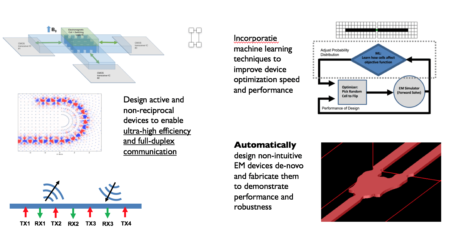
Unfortunately, modeling and designing new SP devices can be quite challenging due to the fact that they often span many wavelengths while having distinct feature sizes smaller than an individual wavelength. This makes lumped-model and ray-tracing approximations inaccurate and the full-wave Maxwell’s equations must be numerically solved for determining the behavior and performance of a device. We are interested in developing new computational approaches for efficiently and accurately modeling SP devices and systems and furthermore coupling them with optimization algorithms to automatically design new, cutting-edge devices only given a high-level goal performance specification and without any human intervention.
We are also interested in developing integrated photonic systems which can enable optical computation, such as fully-optical neural networks.

Computational Electromagnetics
Computational power has increased tremendously over the past couple decades. Compute servers with hundreds of CPU cores and virtually unlimited amounts of memory are now readily available, even at the consumer level. We strive to leverage these significant improvements with computation, coupled with innovative numerical methods, to aid with the modeling and design of novel, non-nonintuitive electromagnetic devices across a wide range on the electromagnetic spectrum.
Our primary modeling goals are driven by the need for extremely fast, yet accurate, simulation techniques for analyzing intricate large-scale systems such as biological tissues, silicon photonic chips, and RF devices.
In the optimization space, we work towards designing algorithms capable of automatically designing robust, ready-to-fabricate electromagnetic devices without any user input except for high-level design performance targets and fabrication constraints.